Why Transistors Still Shape the Future of Electronics
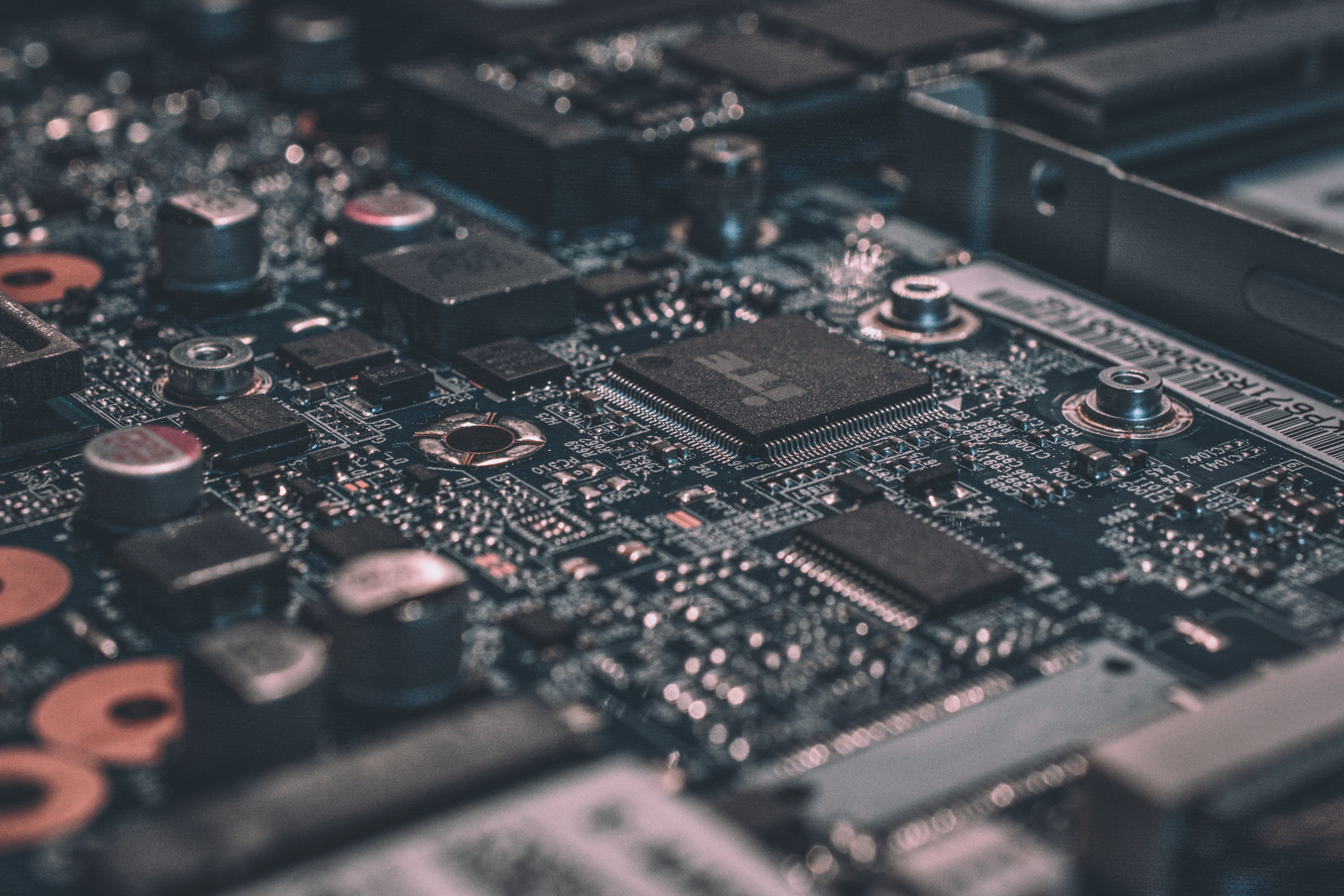
A smartphone, a laptop processor, a data-center accelerator and a simple electronic thermostat all rely on the same fundamental idea: controlling the movement of electrical charge. The transistor is the device that makes this control practical at enormous scale. It can act as a switch, regulate a current or amplify a signal, depending on its design and the circuit in which it operates.
The first successful point-contact transistor demonstration at Bell Telephone Laboratories in December 1947 marked a major turning point in electronics history. John Bardeen and Walter Brattain demonstrated transistor action in germanium; William Shockley subsequently developed the theory and design of the junction transistor. The historical record is more nuanced than a single-inventor story, because several researchers and later manufacturing advances helped turn the discovery into a practical technology (Computer History Museum).
Today, the central question is no longer simply how to make transistors smaller. It is how to make billions of them work reliably, quickly and efficiently while keeping fabrication costs, power demand and heat under control. That distinction helps explain both the industry's progress and its remaining engineering challenges.
The central insight: A smaller transistor does not automatically produce a better device or a more efficient computer. Performance depends on the complete combination of transistor structure, circuit design, interconnects, manufacturing yield, cooling and workload.
1. From a Single Transistor to Billions on One Chip
Early transistors offered an alternative to vacuum tubes, which were comparatively bulky and could consume substantial power. But the transistor's broader impact came from making electronic functions easier to miniaturize and reproduce.
The next major step was integrated-circuit manufacturing. Rather than assembling a circuit from separately packaged components, engineers developed methods for creating multiple devices and their connections on a semiconductor substrate. Jack Kilby's early work and Robert Noyce's monolithic integrated circuit approach were distinct contributions to this evolution. Noyce's approach, based on the planar manufacturing process, helped establish a practical route to producing interconnected components on a single chip (Computer History Museum).
In 1965, Gordon Moore described a trend toward rapidly increasing component counts in integrated circuits. His original projection and subsequent revisions became associated with Moore's Law. The familiar shorthand of transistor counts doubling roughly every two years reflects a historical industry trend, not a physical law or a guarantee that every chip will follow the same schedule (Computer History Museum).
This distinction matters today. A chip may contain more transistors without delivering a proportional increase in application speed. The outcome depends on how those transistors are organized, the data that must move between them, memory performance, software and the amount of power the system can dissipate.
2. How Transistors Control Electrical Signals
Semiconductors such as silicon can be engineered to conduct electricity in controlled ways. Adding carefully selected impurities, a process known as doping, creates n-type or p-type regions with different charge-carrier characteristics. Device geometry and electric fields then determine how current flows through a transistor.
Bipolar junction transistors
A bipolar junction transistor (BJT) uses three semiconductor regions arranged as NPN or PNP. In its forward-active operating region, a relatively small base current can control a larger collector current. BJTs remain useful in analog amplification, current-reference circuits and selected radio-frequency applications, where their characteristics can be advantageous.
The relationship between base current and collector current is often approximated as a current gain, commonly written as beta (β). This is not a fixed universal constant: it varies with the specific device, current, temperature and operating conditions.
Field-effect transistors
A field-effect transistor (FET) controls current through an electric field. In a metal-oxide-semiconductor FET (MOSFET), an insulated gate controls a conductive channel between the source and drain. Ideally, the insulated gate draws very little steady-state DC current, although real devices still have leakage and consume energy when their capacitances are charged and discharged.
MOSFETs are central to modern digital logic. Complementary metal-oxide-semiconductor (CMOS) circuits combine n-channel and p-channel MOSFETs so that, in a stable logic state, one network is designed to be off while the other establishes the output level. This arrangement helps limit static power consumption, although leakage means real circuits do not consume zero power (IEEE Technology Navigator).
| Device type | How it is controlled | Typical strengths | Important design consideration |
|---|---|---|---|
| BJT | Base-emitter drive controls collector current in the relevant operating region. | Useful analog behavior and strong transconductance under suitable conditions. | Requires base drive; operating limits depend on the individual device. |
| JFET | Gate voltage controls a channel through a reverse-biased junction. | High input impedance and low-noise options for selected circuits. | Operating range, polarity and gate limits vary by device. |
| MOSFET | An insulated gate's electric field controls the channel. | Low gate-drive power in steady state and broad use in switching and integrated logic. | Gate charge, on-resistance, leakage, switching losses and thermal limits matter. |
These are qualitative comparisons, not universal component specifications. Voltage, current, gain, switching speed and thermal limits must be checked in the datasheet for the exact part number and operating conditions.
3. What a Transistor Does in an Amplifier
A transistor does not create energy from nothing. In an amplifier, a small input signal controls energy drawn from a power supply. The circuit uses that controlled energy to produce a larger output signal.
Consider a simplified common-emitter BJT circuit with a supply voltage, a collector resistor and a transistor operating in its forward-active region. A first-order DC relationship is:
Here, VCC is the supply voltage, IC is collector current, and RC is the collector load resistance. If the transistor current increases, the voltage drop across the resistor increases and the collector output voltage falls. The output is therefore inverted relative to small input changes in this configuration.
The equation describes a simplified operating relationship, not a complete amplifier design. The actual output depends on biasing, load, transistor characteristics, temperature and whether the transistor remains in its intended operating region. If the transistor is driven into cutoff or saturation, the linear approximation no longer describes its behavior accurately.
For digital circuits, the objective is different. Transistors are arranged to represent logical states, and switching behavior matters more than faithful reproduction of a continuously varying signal. The same broad device family can therefore support very different applications through circuit-level design.
4. Why Shrinking Transistors Is Becoming More Difficult
As transistor dimensions shrink, engineers face several interacting constraints. A smaller channel can help improve density and switching performance, but it also becomes harder to control the channel reliably using the gate alone.
In short-channel devices, the source and drain can exert a greater influence on the channel than intended. Leakage and threshold-voltage behavior become more difficult to manage. At extremely small dimensions, quantum-mechanical effects, including tunneling, can contribute to leakage. Resistance in contacts and interconnects, variability in manufacturing and heat removal also become increasingly important.
This is why a process node name such as “3 nm” should not be interpreted as a promise that every transistor feature measures three nanometers. Node names are technology-generation labels; actual dimensions vary across device features and manufacturers. Comparisons based only on the node label can therefore be misleading.
5. FinFETs and Gate-All-Around Designs
FinFET: controlling the channel from multiple sides
A FinFET raises the channel into a fin-like structure so the gate can control it from multiple sides. Compared with an older planar design, this geometry can improve electrostatic control and reduce unwanted channel leakage under suitable conditions. FinFETs became an important architecture for advanced logic manufacturing.
Gate-all-around: surrounding the channel
Gate-all-around (GAA) transistors take the idea further by surrounding the channel with the gate. One implementation uses stacked nanosheets, which can offer designers more flexibility in balancing drive current, cell area and electrostatic control. Semiconductor research organization imec describes GAA nanosheet devices as a key architecture for advanced logic technology (imec).
These structures are not a simple, universal cure for scaling problems. They introduce manufacturing and integration challenges of their own, and the best choice depends on the required performance, power, area, process maturity and cost. The practical advance is improved control over the channel, not the elimination of all physical limits.
6. The Hidden Cost of Performance: Power and Heat
More transistors and higher clock speeds can increase the amount of computation a chip performs, but they also create a power-management challenge. In CMOS logic, dynamic power is commonly approximated by:
In this expression, α represents switching activity, C is the effective switched capacitance, V is supply voltage and f is switching frequency. The relationship shows why voltage reduction can be especially effective: dynamic power scales approximately with the square of voltage, assuming other factors remain constant (IEEE Technology Navigator).
This equation is a model, not a complete power estimate. Real chips also consume static power through leakage and incur energy costs in clock networks, memories, interconnects and input/output circuitry. Lowering voltage may also reduce maximum stable operating frequency, so engineers must balance energy efficiency against performance.
Heat is the system-level consequence of power dissipation. If a chip cannot transfer heat to its surroundings quickly enough, temperature rises and the system may reduce clock frequency or voltage to remain within safe limits. As a result, an architecture that briefly reaches a high peak speed may deliver less sustained performance than one designed for a better thermal balance.
7. Beyond Silicon: Promise and Practical Limits
Researchers are investigating alternatives and additions to conventional silicon technology, including carbon nanotubes and two-dimensional semiconductors. Such materials may offer useful electrical or scaling properties, but promising device measurements are only one step toward a commercial technology.
A manufacturable transistor also needs repeatable fabrication, reliable contacts, controllable material interfaces, integration with existing processes and competitive production yields. The device must work as part of a complete circuit and remain stable under operating conditions. These requirements help explain why a laboratory demonstration does not automatically translate into a replacement for silicon CMOS.
Graphene deserves a particular qualification. Its excellent conductivity does not, by itself, make it an easy replacement for silicon in conventional digital logic: graphene lacks the natural bandgap generally needed for a transistor to switch sharply between a low-current off state and a high-current on state. Other two-dimensional semiconductors may have more suitable band structures, but manufacturing and integration hurdles remain.
The likely future is not necessarily one material replacing silicon everywhere. Different technologies may serve different roles, while progress also comes from better transistor architectures, advanced packaging, specialized accelerators and more efficient system design.
8. What These Developments Mean for Consumers
The details of transistor architecture are rarely visible on a product box, but the consequences can affect everyday use. A useful comparison should focus on the performance a device can sustain for the work it is expected to do.
- For laptops: Consider battery life, sustained performance, fan noise and performance under prolonged workloads, not only the advertised processor generation.
- For phones: Camera processing, gaming performance, modem efficiency and thermal behavior depend on the complete system-on-chip and software, not transistor density alone.
- For electronics projects: Choose a transistor using its datasheet. Check maximum voltage, current, power dissipation, safe operating area, gate or base drive, switching behavior and heat-management needs.
- For sustainability: Efficiency per task and product lifetime matter alongside peak performance. A more advanced chip does not automatically make the whole device more environmentally responsible.
These are practical consequences of transistor engineering, rather than a claim that one process node or transistor type is best for every product. The appropriate design depends on the task, constraints and cost.
Conclusion: Progress Is Now a System-Level Challenge
Transistors transformed electronics by making reliable switching and amplification possible in compact solid-state devices. Integrated circuits then turned that device-level breakthrough into an industrial platform for computers, communications and consumer electronics.
The next phase of progress will not be measured by size alone. FinFET and gate-all-around architectures improve control over shrinking channels, while power management, interconnects, manufacturing yield, materials and thermal design increasingly shape the final result. The central engineering challenge is to make the whole system faster or more capable without exceeding its energy, reliability and cost limits.
For readers and consumers, that is the most useful way to interpret semiconductor advances: the newest transistor architecture matters, but what ultimately counts is how effectively it turns electrical energy into dependable, useful computation.
References and Further Reading
- Computer History Museum. (n.d.). 1947: Invention of the Point-Contact Transistor. The Silicon Engine. https://www.computerhistory.org/siliconengine/invention-of-the-point-contact-transistor/
- Computer History Museum. (n.d.). 1959: Practical Monolithic Integrated Circuit Concept Patented. The Silicon Engine. https://www.computerhistory.org/siliconengine/practical-monolithic-integrated-circuit-concept-patented/
- Computer History Museum. (n.d.). 1965: "Moore's Law" Predicts the Future of Integrated Circuits. The Silicon Engine. https://www.computerhistory.org/siliconengine/moores-law-predicts-the-future-of-integrated-circuits/
- IEEE Technology Navigator. (n.d.). CMOS. https://technav.ieee.org/topic/cmos/
- IEEE Technology Navigator. (n.d.). Power Dissipation. https://technav.ieee.org/topic/power-dissipation/
- imec. (n.d.). Outer-wall forksheet: Bridging nanosheet and CFET. https://www.imec-int.com/en/articles/outer-wall-forksheet-bridge-nanosheet-and-cfet-device-architectures-logic-technology